Mixed Signal Microelectronics
From Intelligent Materials and Systems Lab

Why CMOS-MEMS?
- Reduced Parasitic degradation
- Mainstream processes:High volume production
- Most scalable and monolithic
- Targeted for consumer electronics (primarily)
- Less degrees of freedom (Not the best solution!)
Our Vision
We strive to adapt and develop smart ways for our MEMS materials in standard CMOS technology for optimized ASIC design targeted for biomedical and consumer applications.
Capabilities
Methodology
Typically, we follow the standard procedure to develop our devices:
- Device design, Modeling and Optimization
- Black-box modeling and co-simulation with electronics (transistor-level design)
- Device Fabrication and Tape-out (corresponding to the technology node)
- Characterization (in terms of ambient and electrical factors) for optimal operation
- Convergence of modeling and experimental results for validation
- A Typical workflow for CMOS MEMS Pressure sensor
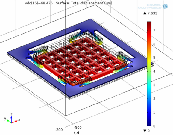
FEM of CMOS-MEMS resonator at Pull-in
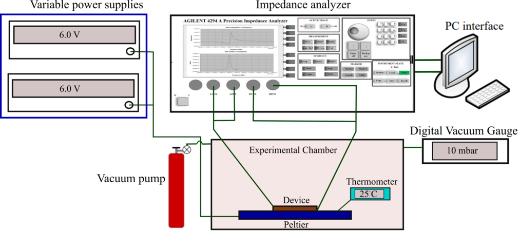
Block diagram of experimental set-up for device characterization
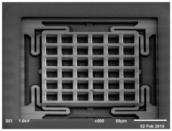
View of Monolithic CMOS-MEMS Pressure sensor under scanning electron microscope


Tools we use
Software
- Modeling and Optimization: MATLAB, COMSOL Multiphysics
- Transistor level Design and Layout: Cadence
Equipment
- SEM
- FIB
- Microprobe setup
- Impedance Analyzer
Primary contacts
Saoni Banerji postdoc researcher of CMOS MEMS sensors
Alvo Aabloo professor, head of the IMS lab
Student projects
Possible topics for BSc and MSc level students
Portfolio
Research Topics
Possible interesting topics are:
- MEMS-Based Sensors for Human Centered Applications (CMOS MEMS Based Micro Biotronics)
- Monolithic sensors in CMOS technologies (targeted towards consumer electronics)
Selected Publications
- S. Banerji, D. Fernández and J. Madrenas, (2018) A Comprehensive High-Level Model for CMOS-MEMS Resonators, in IEEE Sensors Journal, vol. 18, no. 7, pp. 2632-2640, April 1, 2018.
- S. Banerji, D. Fernández and J. Madrenas, (2017) Characterization of CMOS-MEMS Resonant Pressure Sensors, in IEEE Sensors Journal, vol. 17, no. 20, pp. 6653-6661, Oct.15, 2017.
- S. Banerji, P. Michalik, D. Fernández, J. Madrenas, A. Mola, J. Montanyà,(2017) CMOS-MEMS resonant pressure sensors: Optimization and validation through comparative analysis, , Microsyst. Technol., vol. 23, no. 9, pp. 3909-3925, 2016.